Portable Optical Precision Profilometer for Chip-level Metrology Applications
Overview
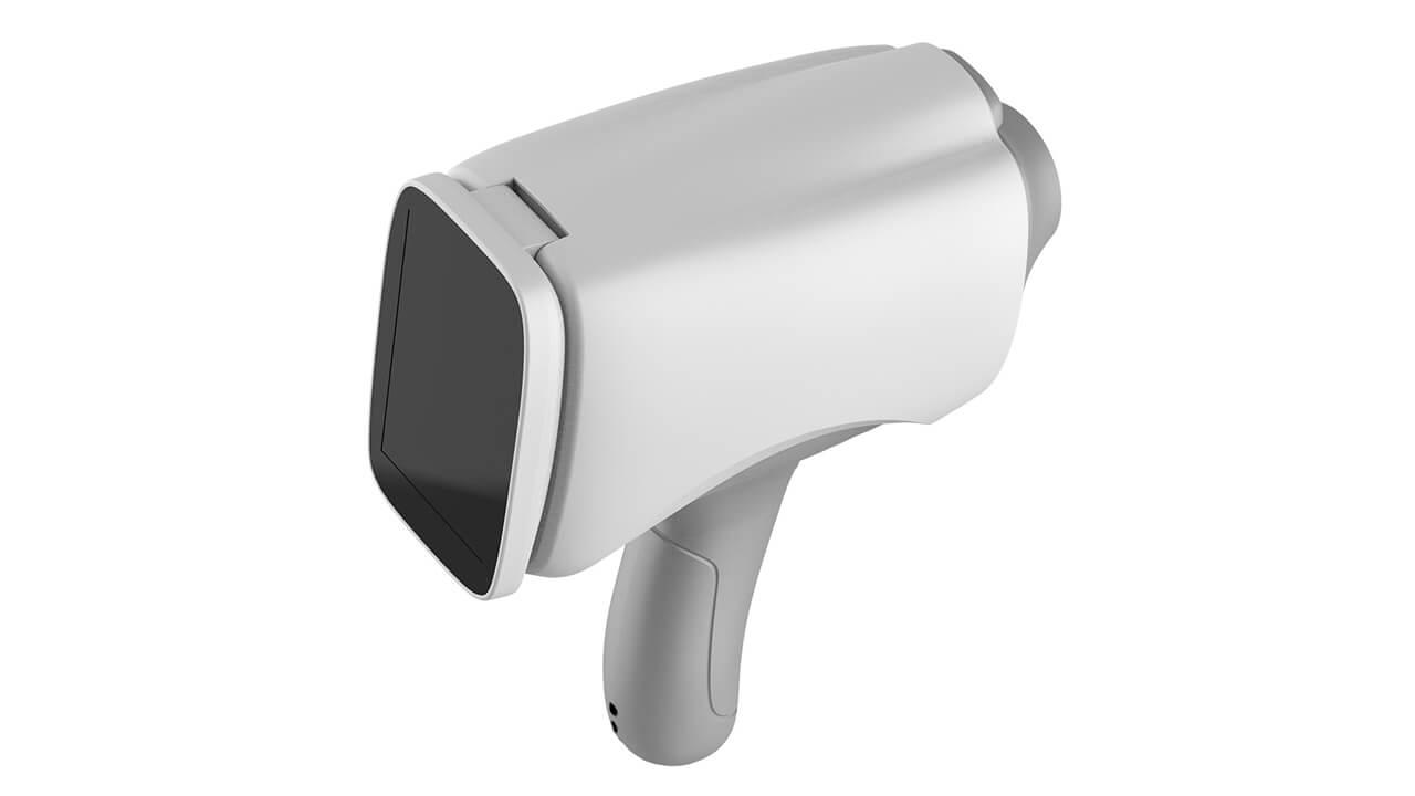
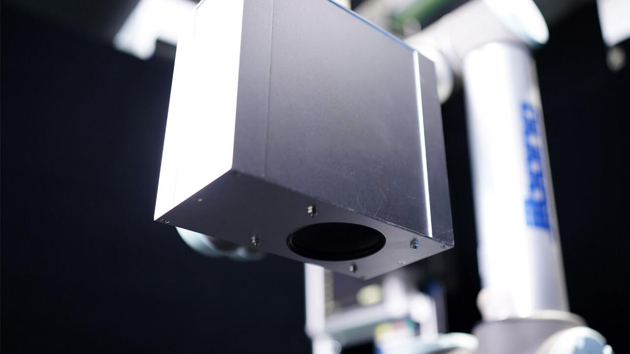
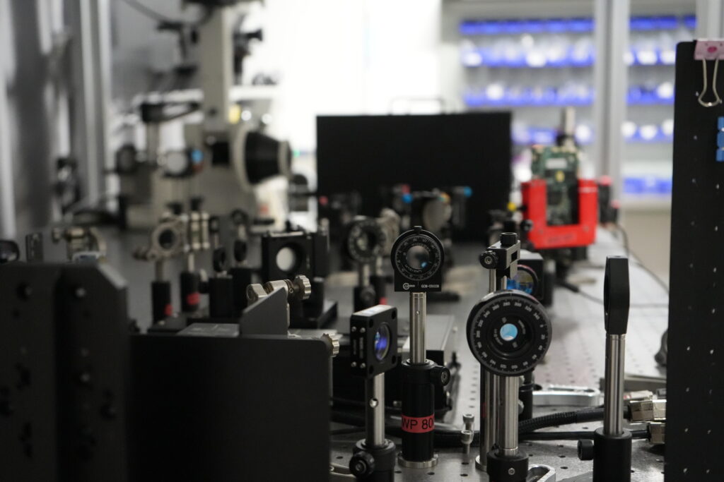
We have developed a low-cost portable optical precision profilometer (POPP) with a compact size of around 30 cm x 20 cm x 10 cm. The system is based on a novel common-path quantitative phase microscopy method, which allows to achieve < 1 nm measurement precision and < 10 ms measuremnt time.
Technical name of innovation
Portable Optical Precision Profilometer (POPP)
Research completion
2021/6/30
Commercialisation opportunities
Exclusive licensing
Problem addressed
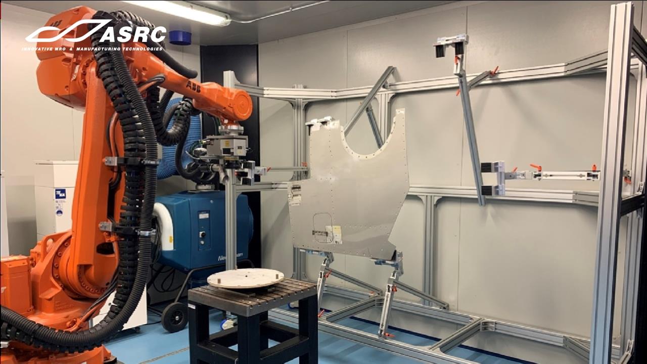
In recent years, advanced manufacturing and chip fabrication geatly demand for high precision, low-cost and integratable inspection tools. However, there is a large market shortage of such tools. Therefore, we developed portable optical precision profilometer (POPP) and demonstrated its applications for material metrology and chip inspection.
Innovation
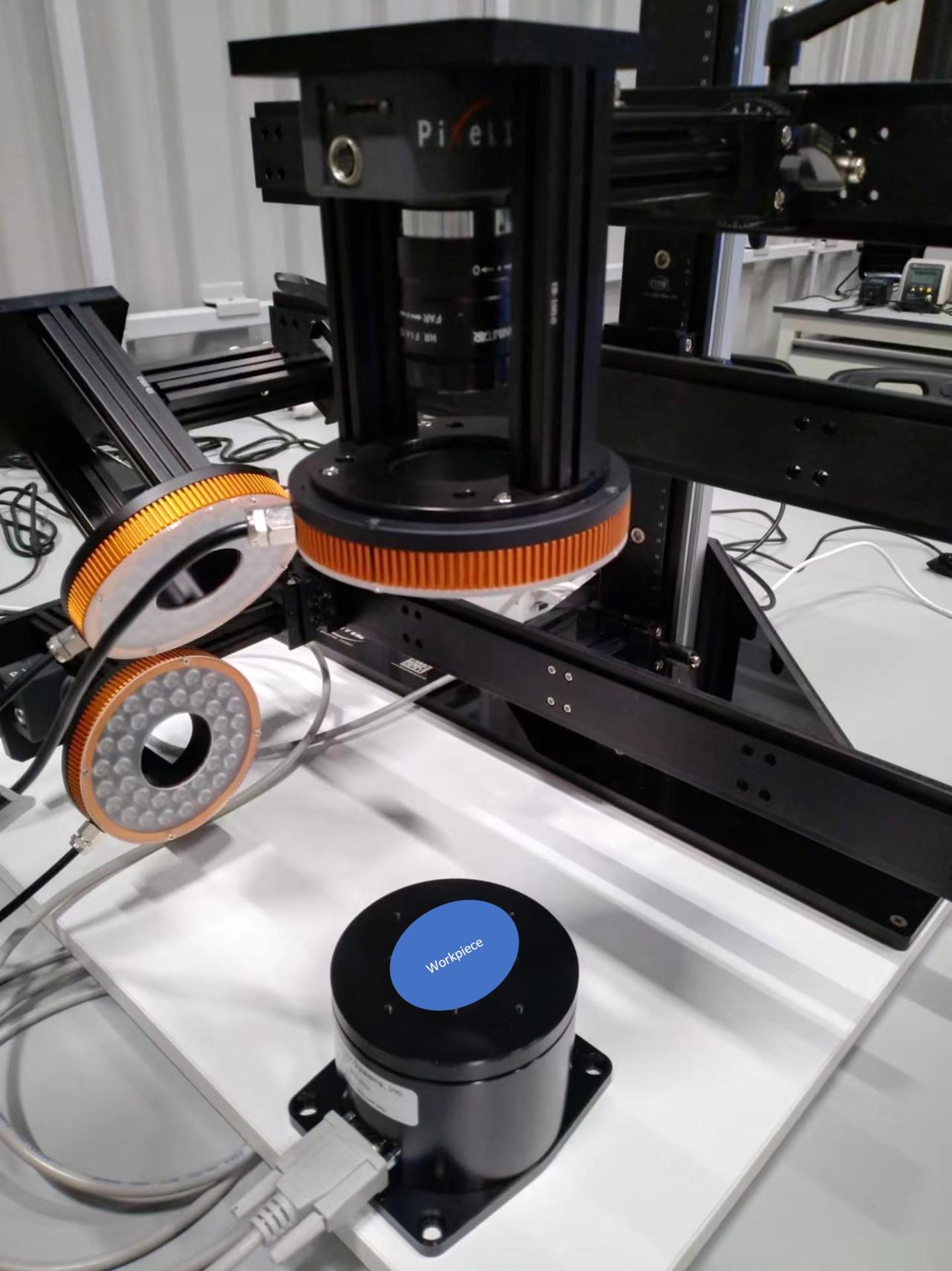
- The compactness of the POPP system is enabled by a new illumination design and a customized microscopic imaging system.
- The POPP system uses a novel common-path interferometer to realize real-time imaging amd high precision measurements.
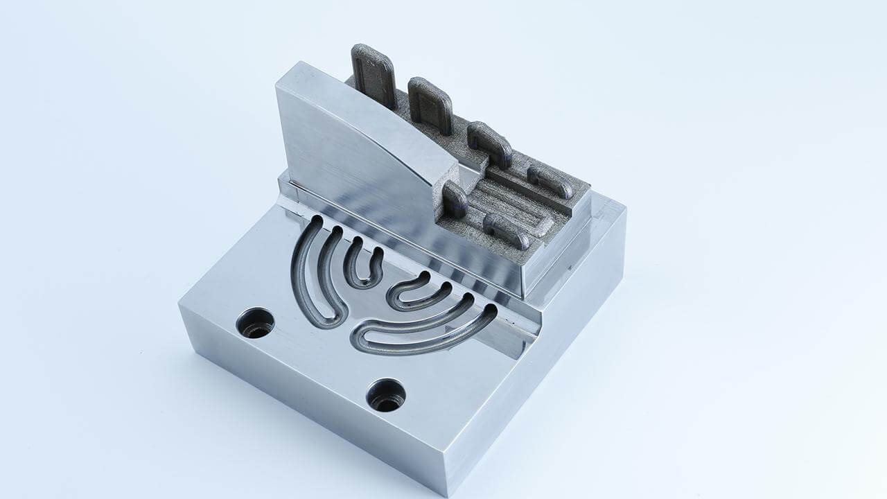
- We have widely realized profiling of various chip structures, including flexible electronics, 0.5-50 micron particles, microfludic chips,etc.
Key impact
- The POPP system has achieved a compact dimension, as well as high technical specifications for sample measurements, including: (1)< 1 nm measurement sensitivity; (2) maximum height measurement range of 50 micron; (3) better than 0.5 micron imaging resolution; and (4) switchable field of view.
- Through collaborations with research labs and companies, we have tested various chip samples and performed analysis, thus demonstrating POPP system's great potential in chip-level metrology applications.
Award
- "Portable Dynamic Surface profilometer" won the 2nd place (top 6 over 194 teams) in the Hong Kong and Macau Division at the 11th Shenzhen Innovation and Entrepreneurship Competition/the 1st Shenzhen Virtual University Innovation and Entrepreneurship Competition.
- Our project won the "New Talent of the Year" in the first MIT Technology Review China Life Science Entrepreneurship Competition.
Application
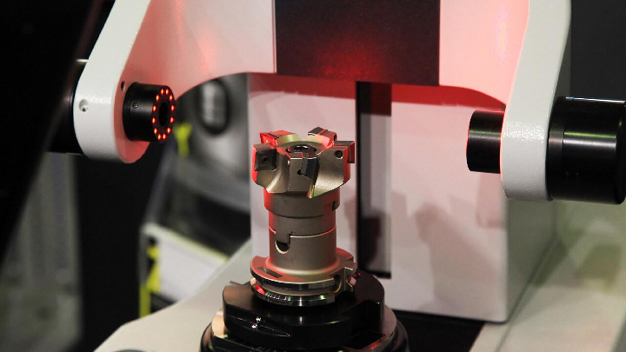
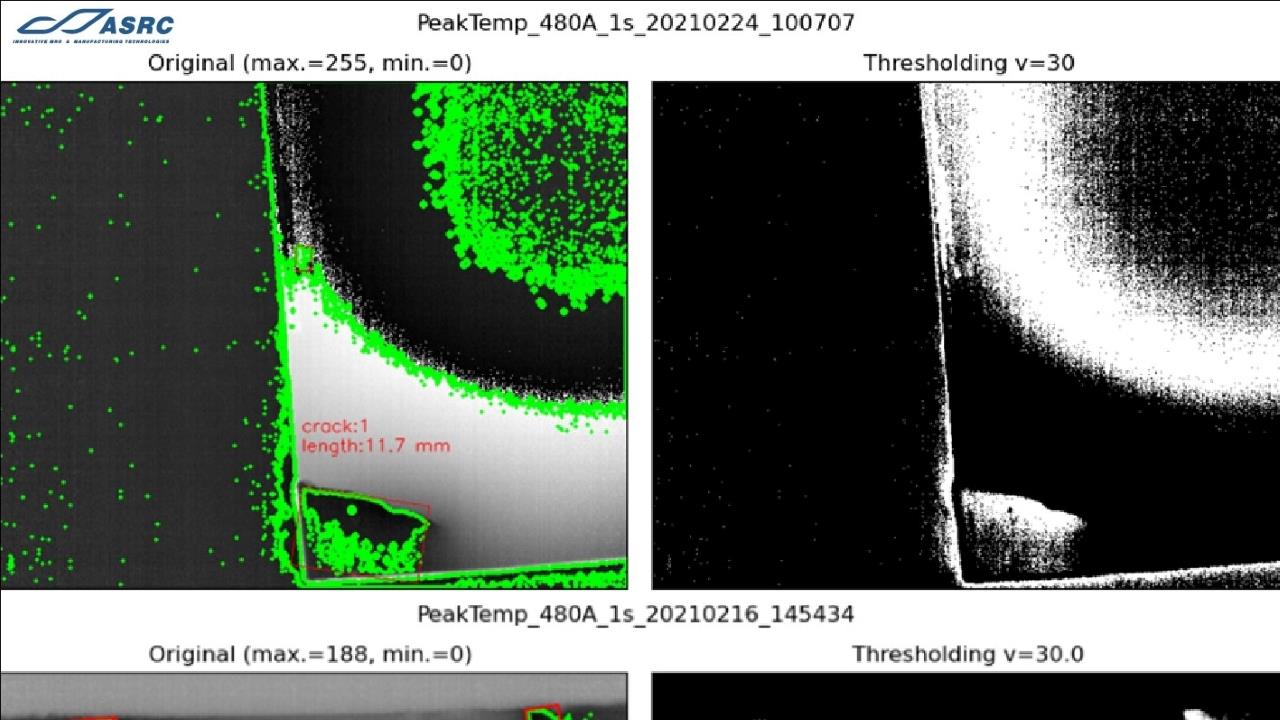
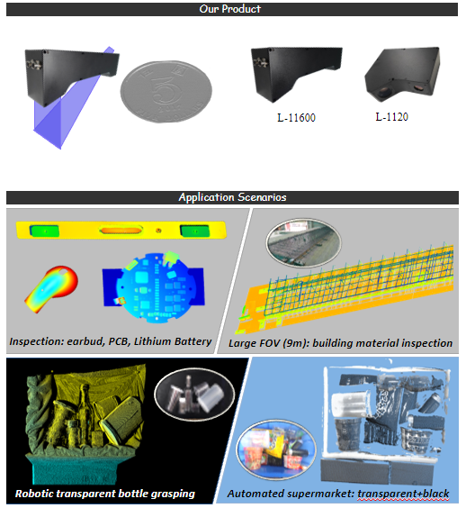
- Electronic device characterization, including defective micro-lens detection on image sensors and saw mark and crack detection of sliced chips
- Characterization of flexible electronics
- Microscale particle sizing, e.g. >0.5 μm particle sizing on different substrates
- Biochip characterization,such as microfluidic devices
Patent
- US Non-Provisional Patent Application, Serial No. 16/917,216.
- China Invention Patent, Application Number: 202010907562.X.
The Chinese University of Hong Kong (CUHK)
Founded in 1963, The Chinese University of Hong Kong (CUHK) is a forward-looking comprehensive research university with a global vision and a mission to combine tradition with modernity, and to bring together China and the West. CUHK teachers and students hail from all around the world. Four Nobel laureates are associated with the university, and it is the only tertiary institution in Hong Kong with recipients of the Nobel Prize, Turing Award, Fields Medal and Veblen Prize sitting as faculty in residence. CUHK graduates are connected worldwide through an extensive alumni network. CUHK undertakes a wide range of research programmes in many subject areas, and strives to provide scope for all academic staff to undertake consultancy and collaborative projects with industry.
Enquiry