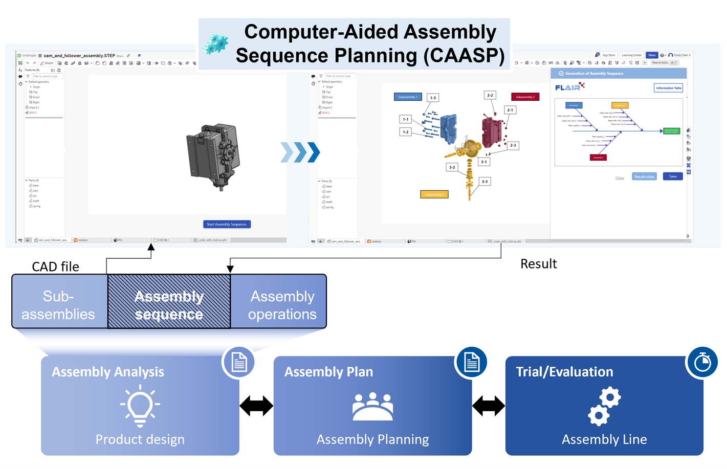
Co-axial Line-scan Confocal Technology for Semiconductor Inspection
Overview
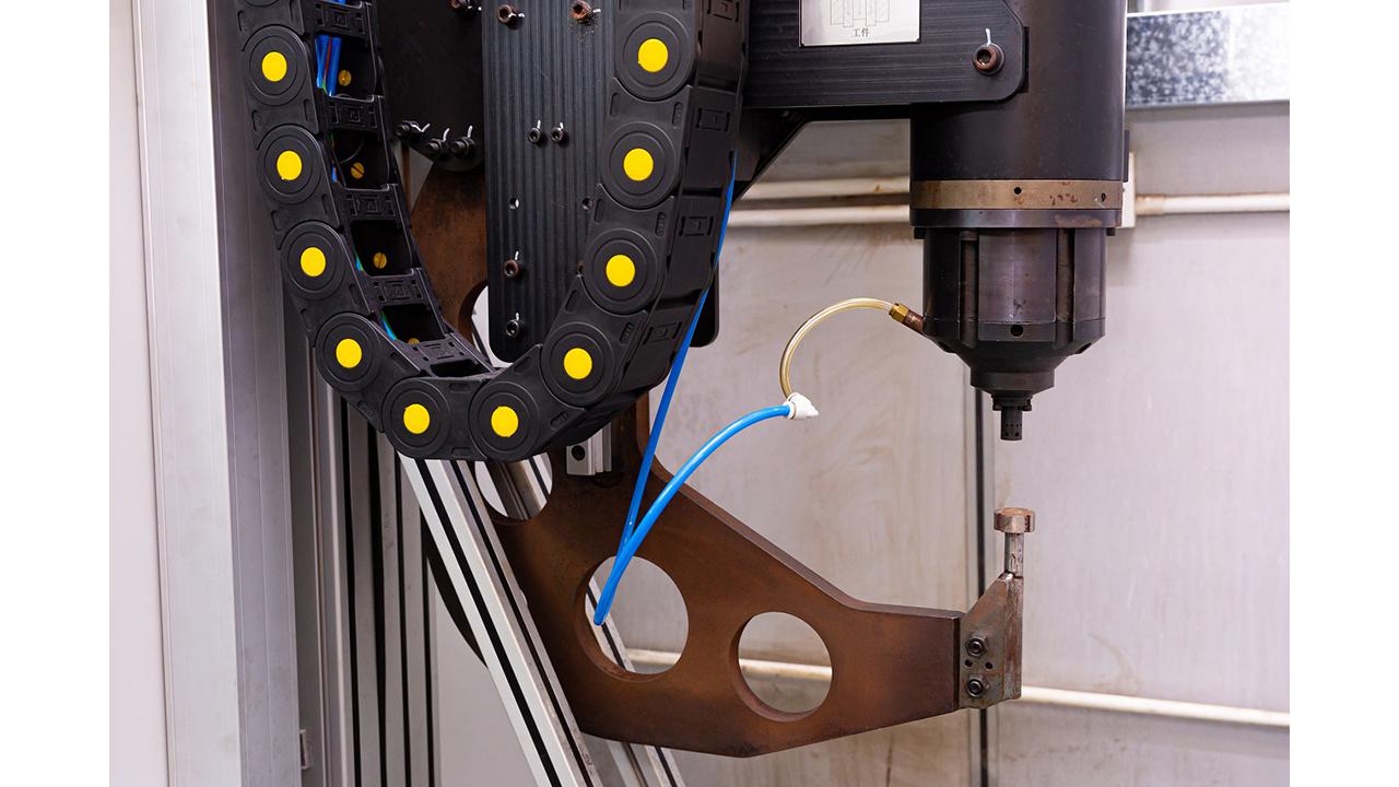
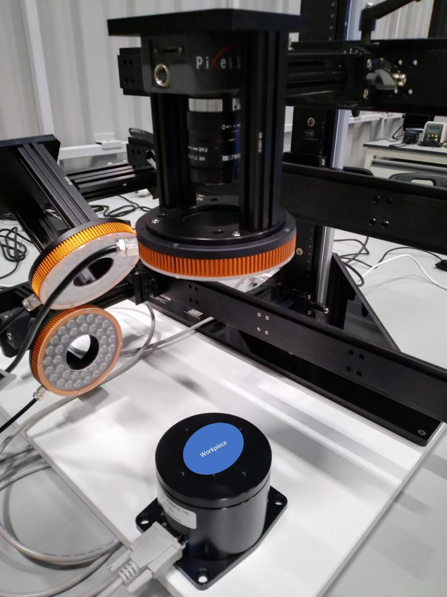
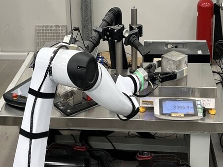
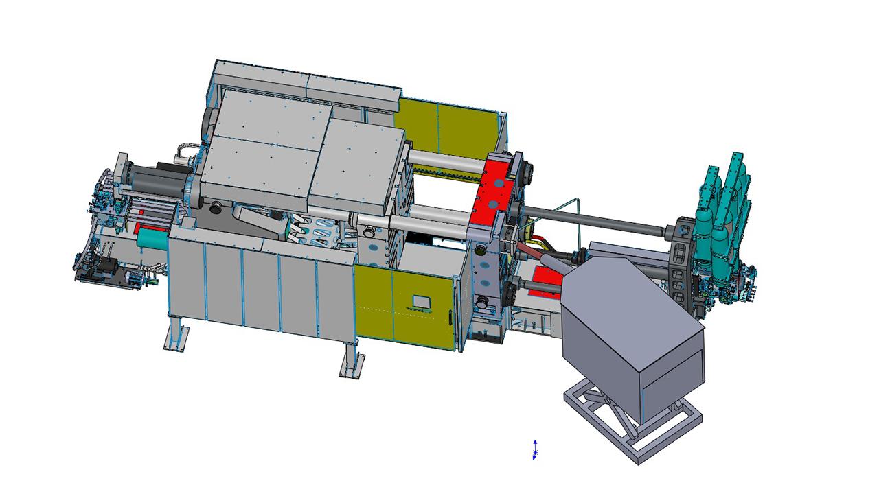
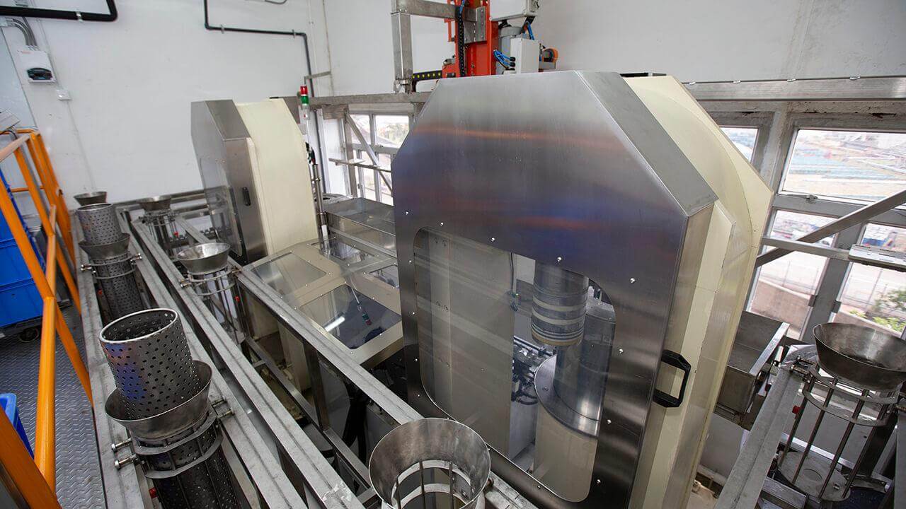
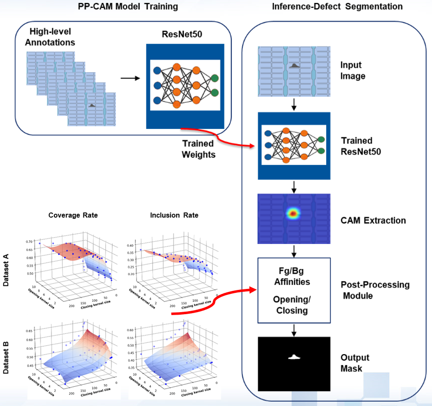
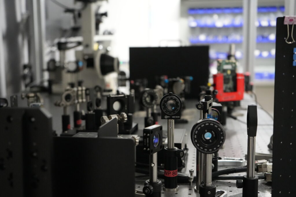
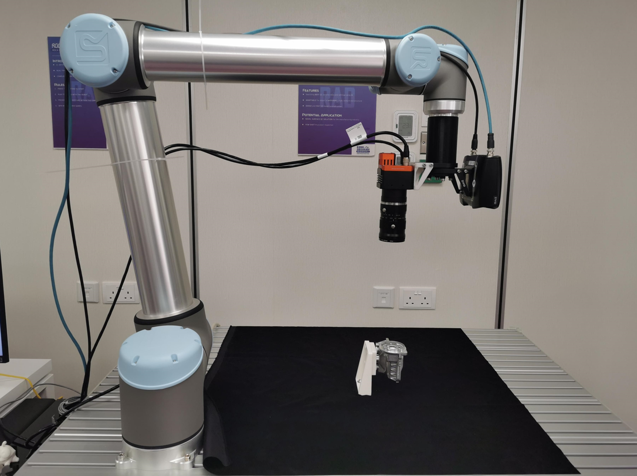
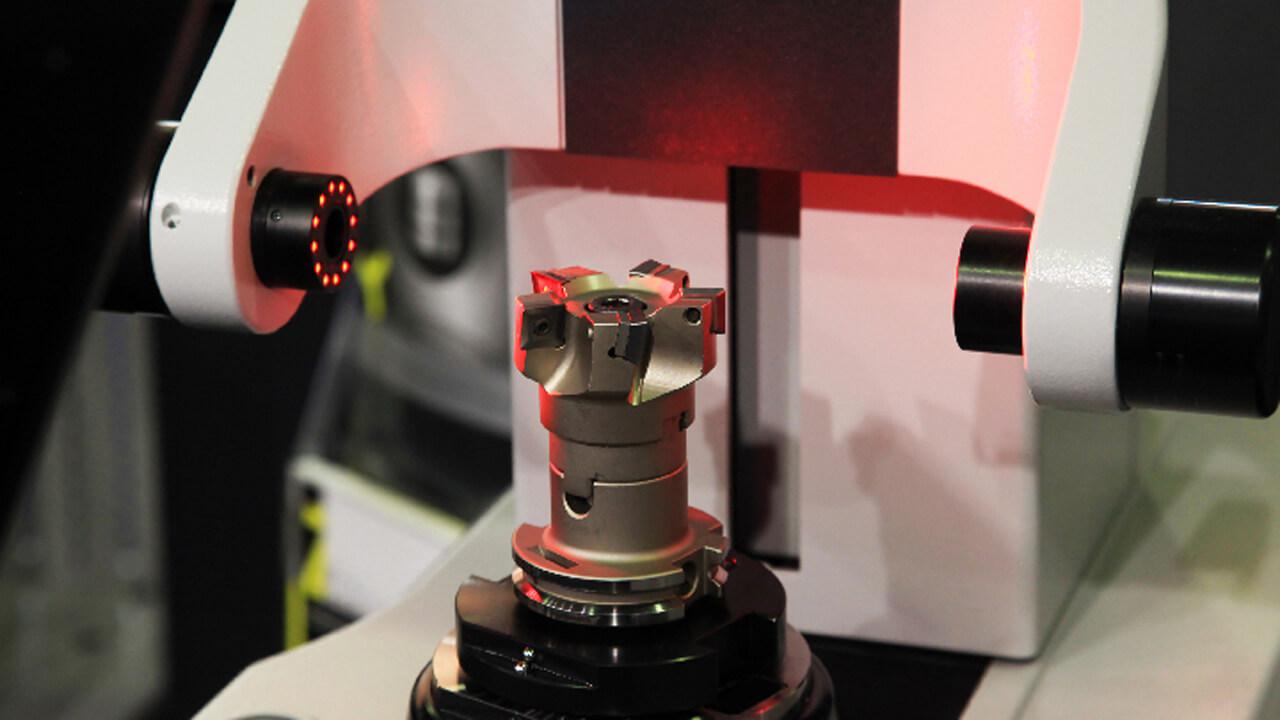
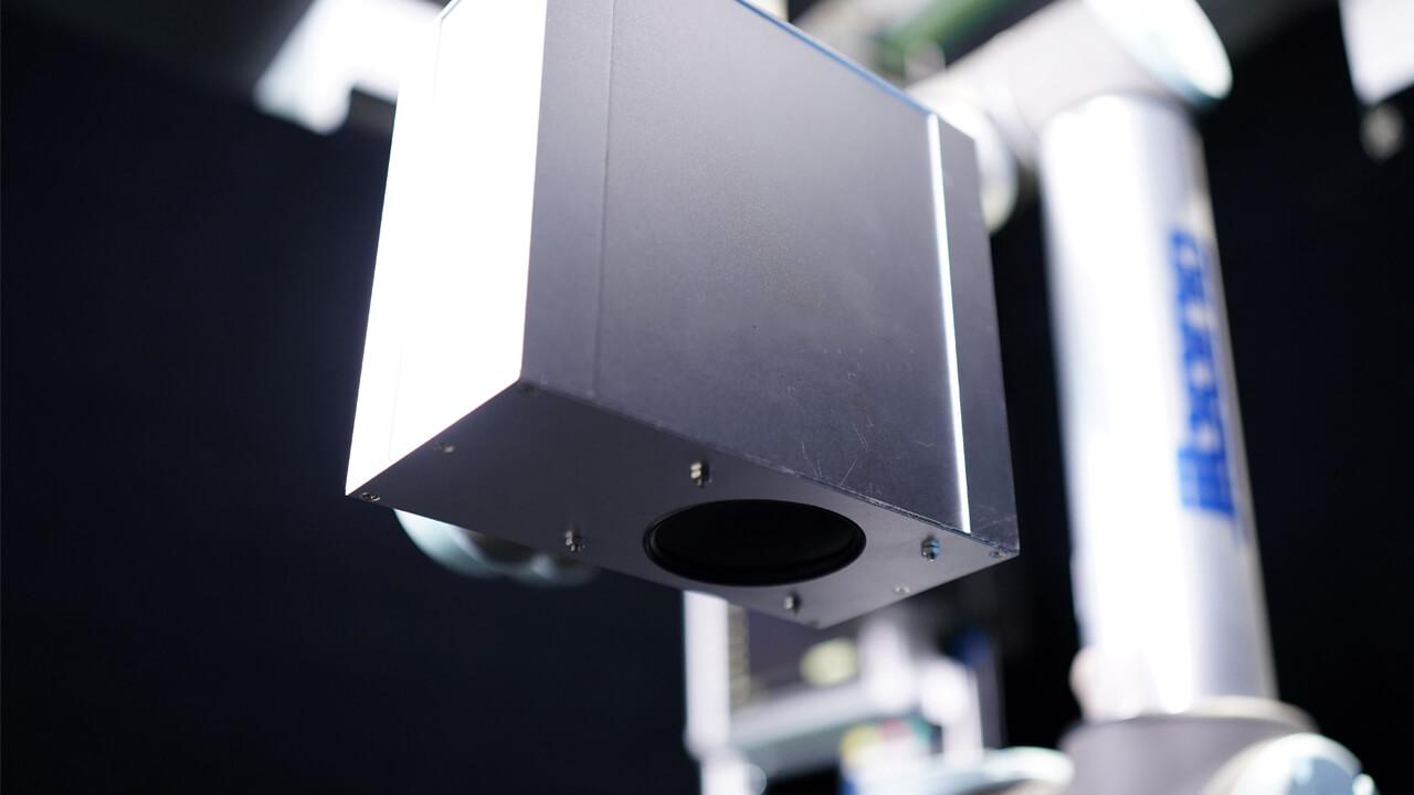
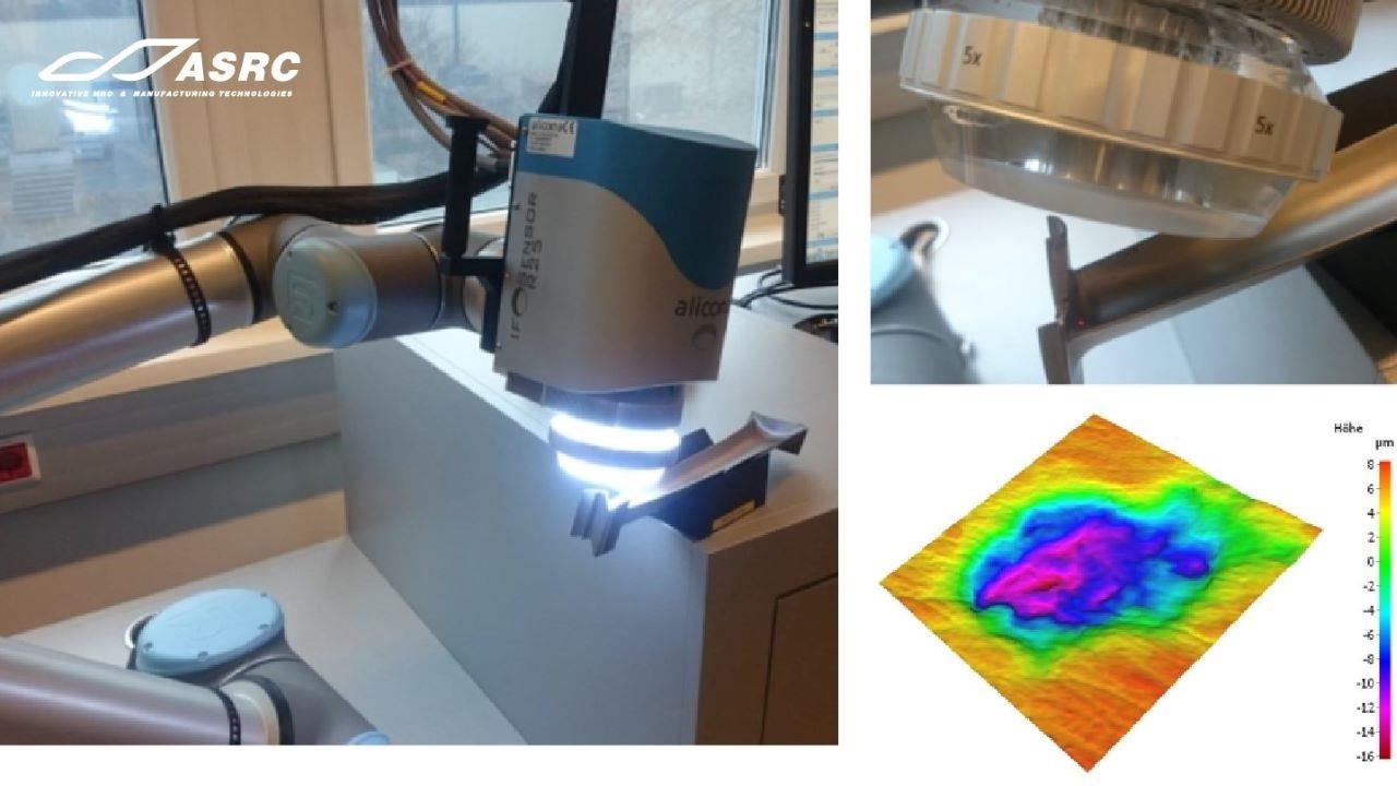
This is a high-speed and high-resolution coaxial confocal line-scan system, used for inspection in semiconductor and electronics industry. It offers a high resolution down to 0.5μm along depth direction, an aspect ratio of depth to diameter more than 10:1 in deep hole measuring scenario and a high scanning speed up to 10000 lines/s, effectively addressing the challenges in traditional inspection.
Commercialisation opportunities
IP licensing, Technology co-development, Contract research
Problem addressed
With Moore's Law approaching its limit and the semiconductor processing approaching physical limit, advanced packaging shows great impact on chip performance. More and more stringent requirements are put forward for the in-line semiconductor inspection. Traditional methods have low scanning speed, cannot measure small structures, or only inspect limited defects. This line scanning 3D imaging technology can solve these problems.
Innovation
- The design of the coaxial telecentric optical path enables the system to measure the features with high aspect ratio reaching 8:1-18:1 or above.
- The implementation of hardware acceleration embedded system can make the line scanning speed reach 10000 lines/sec or above.
- Multi-layer algorithm and wavelet transform algorithm is developed to solve the problem of multi-layer interface reflection in transparent object. So that the 3D point clouds of each layer can be clearly obtained.
Key impact
- Able to measure high aspect ratio reaching 8:1-18:1 or above
- High scanning speed up to 10000 lines/s or above
- High resolution down to 0.5μm (along depth direction)
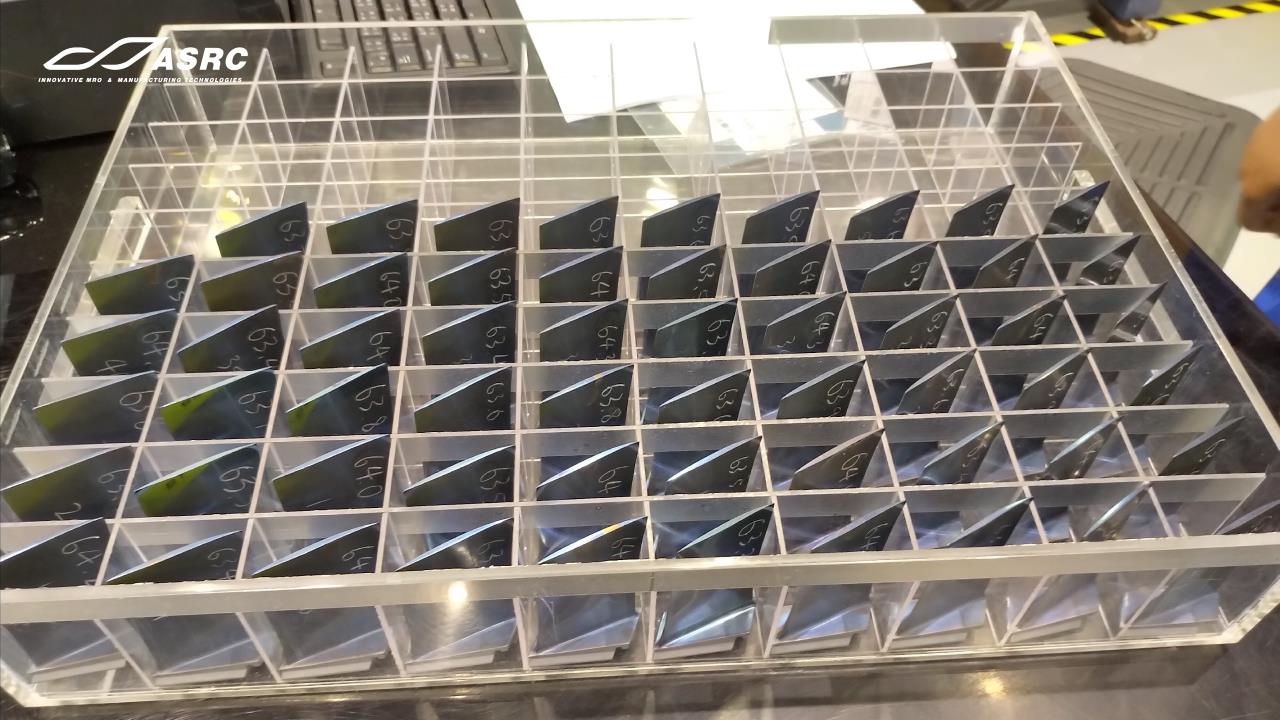
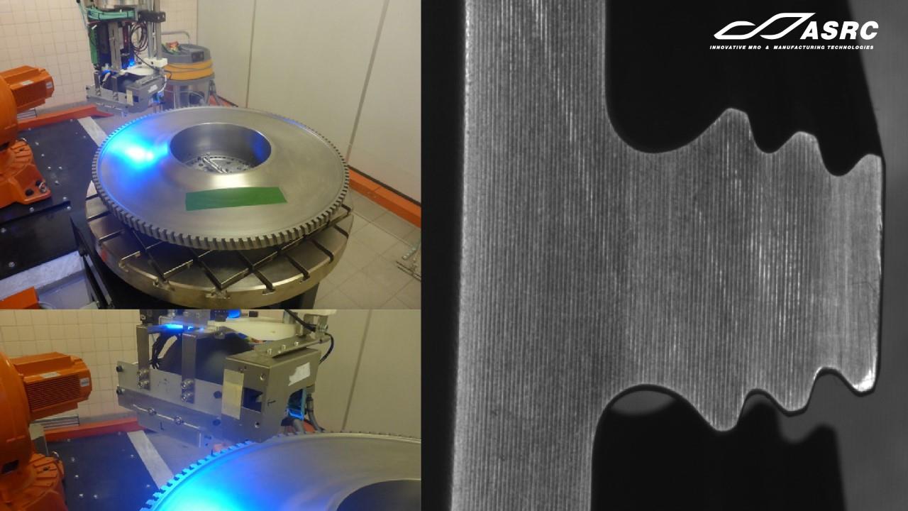
- Able to detect different features, such as wafer bump, redistribution layer (RDL), and through-silicon via (TSV)
Award
- Silver Medal in The 48th International Exhibition of Inventions Geneva
- 2023-2024 Hong Kong Awards for Industries: Equipment and Machinery Design Award
Application
- In-line inspection for advanced packaging in semiconductors: This technology meets the increasing inspection demands for elements such as wafer bump, redistribution layer (RDL), and through-silicon via (TSV).
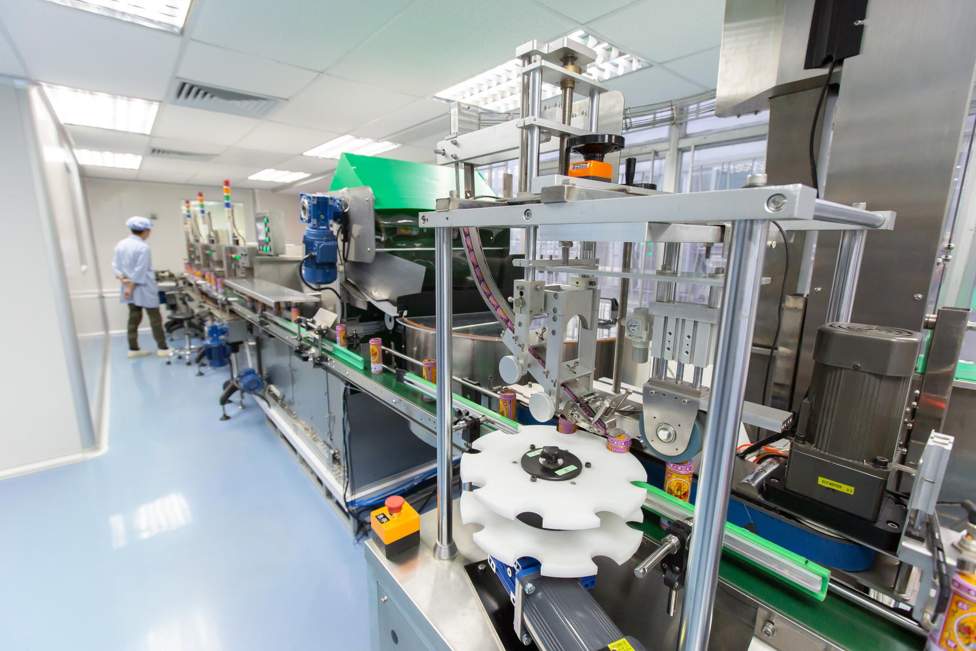
- In-line inspection for electronics and advanced manufacturing: PCB substrate inspection, copper substrate inspection, deep hole measurement, multi-layer transparent object inspection, and mobile phone cover glass inspection.
Patent
- US Patent No. 11,287,626
- US Patent Application No. 19/096,181
Hong Kong Applied Science and Technology Research Institute (ASTRI)
Hong Kong Applied Science and Technology Research Institute (ASTRI) was founded by the Government of the Hong Kong Special Administrative Region in 2000 with the mission of enhancing Hong Kong’s competitiveness through applied research. ASTRI’s core R&D competence in various areas is grouped under four Technology Divisions: Trust and AI Technologies; Communications Technologies; IoT Sensing and AI Technologies and Integrated Circuits and Systems. It is applied across six core areas which are Smart City, Financial Technologies, New-Industrialisation and Intelligent Manufacturing, Digital Health, Application Specific Integrated Circuits and Metaverse.
Enquiry